Flashcards · Oct 2026 · 48 cards
Intel
How the world's most advanced chips are made
Many thanks to Will Michaels for collaborating with me on the research and production of this episode!
Bringing up a new node
A sample is made very thin (less than 100 nanometers). Then, electrons are shot at the sample. Different materials block or scatter the electrons by different amounts. These show up as darker or lighter regions in the image. This technique can visualize features down to the atomic scale.
Lessons from 10 nanometer
- Cobalt interconnects. This material was complex to integrate and hurt yields.
- Multiple patterning. This increased the number of lithography passes and complicated the process substantially.
- Contact over active gate. This decreased the tolerance for misalignment and caused yield issues.
Droplets of liquid tin 25-30 micrometers wide are dropped into a chamber where they are hit by two laser pulses. The first laser pulse reshapes the tin droplet into a flat sheet. Then, a second, higher power, pulse hits the droplet and vaporizes it into a plasma. The electrons in this plasma become excited and emit 13.5 nm light when they lose energy.
From planar to gate-all-around
Top to bottom: gate (metal) on top of an SiO₂ insulator, sitting on a P-type substrate. Two N-doped wells flank the gate on the left and right — the source and the drain. When the gate is positive, a channel of electrons forms in the substrate just under the insulator, connecting source to drain.
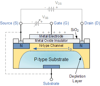
It pulls up the electrons in the P-type substrate, filling up the holes at the top — the channel.
- Planar: gate sits flat atop the source-to-drain channel.
- FinFET: gate drapes the channel from three sides.
- Gate-all-around: gate fully wraps the channel from all sides.
Better gate control means you can shrink the source-to-drain distance (the "gate length") without source/drain fields leaking current through.
The gate consists of several metals that are chosen to optimize the conductivity of the gate and threshold voltage of the device. They can melt and degrade when subjected to high temperature processes that occur at the beginning of transistor fabrication. Therefore, they are deposited last to avoid these high temperature steps.
As transistors got smaller, silicon dioxide would let too much current leak between the gate and the channel. High K metal gates have better capacitance.
Dennard scaling refers to the period from 1960-2005 in which planar MOSFETs were scaled down by directly shrinking their dimensions, which increased power density.
However, threshold voltage and leakage current do not scale with transistor length - Source and Drain got so close together that they would be current even without the channel being on.
The first precursor gas is passed over the wafer. It typically has a metal part and an organic part. The metal portion binds to the surface, forming a single layer with the organic sticking up. This process is self-limiting because binding only happens between the wafer and the metal, not between the metal and the organic. Next, the chamber is purged and the second precursor is introduced. This gas reacts with the dangling organics pulling off the organic part of the molecule and leaving a single atomic layer of the metal. This process is repeated for as many layers as desired.
High-NA EUV and the PDK
NA measures how wide a cone of light the scanner's optics can focus onto the wafer. A wider cone focuses to a smaller spot, so finer features can be printed. Standard EUV has an NA of 0.33; High-NA raises it to 0.55, which prints features about 1.7× smaller (0.55 / 0.33) in a single pass.
1. As the NA increases, the lenses become very large. Large lenses mean that the light will strike the lenses at a large angle. At large angles different polarizations of light are reflected differently. This reduces the contrast between the absorbing and reflecting parts of the mask. 2. The depth of field (DOF) quantifies what thickness of the resist is in focus during exposure. DOF ~ 1 / NA². Therefore, as the NA is increased, the DOF gets smaller, meaning a thinner resist must be used. Thinner resists are worse at blocking subsequent etching steps.
When features are smaller than the scanner can print, the pattern is split across two, three, or even four exposures, each printing a different subset of the features. Every extra pass takes time on a ~$200 million EUV machine and adds another opportunity for defects.
A chip has thick power lines, which deliver electricity to the transistors, and thin signal lines, which must be spaced apart so signals don't interfere. Traditionally both were crammed together in the wiring above the transistors. Backside power moves the power lines below the transistors, to the back of the wafer, so the signal lines on top don't have to be packed as tightly.
Intel uses backside power, which relaxes the wiring pitch on the front side enough to print those layers in a single High-NA pass. TSMC's processes don't have backside power, so their front-side pitches are tighter and would still need multiple passes with High-NA. For them, double-patterned standard EUV is cheaper.
A different tech tree
A complementary field-effect transistor. Today the n-type (NMOS) and p-type (PMOS) transistors are built side by side. A CFET stacks them directly on top of each other, which in principle fits twice as many transistors into the same area.
Heat. Logic consumes far more power than memory, and every stacked layer adds heat that has no clear path to escape.
Ruthenium interconnects
Copper diffuses so much that if it was directly touching the transistor, you'd worry about it damaging sensitive areas. So we used Tungsten there.
Tungsten has higher resistivity, so it would require more power for all the interconnects if we used tungsten all over.
Ruthenium is easier to etch than copper, which allows you to etch out air gaps (air has the lowest capacitance)
At nanoscale, ruthenium has lower resistance, because mean free path of an electron is lower, which means it accumulates and thus dissipates less energy between collisions
- This allows air gaps to be created between interconnects. Air is a very good insulator, so this lowers the capacitance between interconnects when compared to having a dielectric there.
- It simplifies the process compared to making copper interconnects. Depositing and then etching ruthenium is easier than the Damascene process used to make copper interconnects.
Stacking transistors
Connections that used to run on top of (or below) the transistors now have to go vertically between the stacked devices. That requires deep, narrow trenches. High-aspect-ratio etches are difficult, and filling those tiny spaces can leave air gaps or voids that never fill.
Hybrid bonding
In 2.5D, different chips are placed on an interposer. Connections between the chips are run through the interposer. In 3D, the chips are bonded directly to one another through solder bumps or copper connections.
Two chips side by side communicate through their facing edges. Doubling a chip's width and length gives 4× the area for compute but only 2× the edge length for connections. So as transistors get denser, a chip's ability to compute grows faster than its ability to move data, and in AI workloads the data traffic (e.g. between GPU and HBM) is often the bottleneck.
The copper pads of two chips are aligned, pressed together, and heated. The copper expands to bridge the gap and fuses, and the insulating surfaces around the copper bond too. Removing the bulky, resistive solder bumps allows much finer pitch, so connections are denser and shorter. The hard part is alignment and defects, which is why it is only now entering volume manufacturing.
Wafer-to-wafer bonds two full wafers together, so the dies on each must match exactly in size and position, and good and bad dies are paired randomly: some good dies get bonded to bad ones and are wasted. Chip-to-wafer singulates and tests the dies first, so only known good dies are bonded to known good positions. Wafer-to-wafer dominates CMOS image sensors; chip-to-wafer makes more sense for logic-on-logic.
Not covered in the video
A two-terminal semiconductor that allows current to flow one way but not the other.
Insulator.
Electrons saturate the holes in P, leaving no differential for the electrons in N to jump towards. Meanwhile, the extra electrons in N flow back to the battery.
Conductor.
Electrons saturate N, push into the depletion region, then jump across to the holes in P, which then return to the battery.
A large positive current is allowed to flow from collector to emitter.
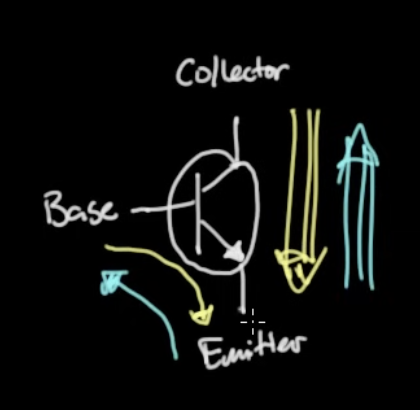
Image from Ben Eater's transistor video.
You're allowing electrons from the emitter to get all the way up into the base, so close that they can jump across the depletion region between base and collector.
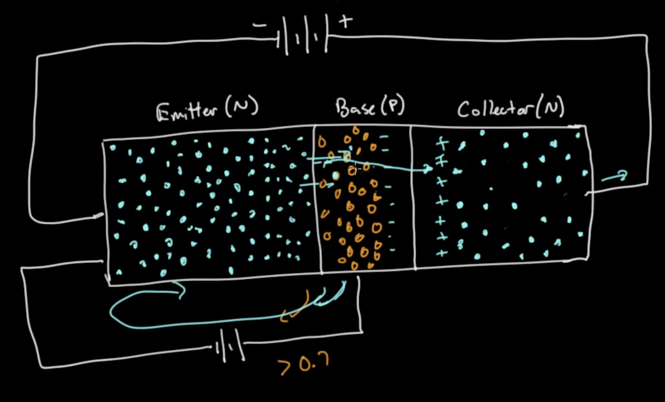
Image from Ben Eater's transistor video.
When switching the device on, these doped regions supply the carriers (electrons or holes) to create the channel. Without the doping here, carriers would have to be generated by the silicon within the channel itself, which could take milliseconds or seconds.
In a MOSFET, the input is a voltage you set. In a BJT, it's a current you must keep feeding.
Thanks to the insulator between the gate and the channel, there's no power dissipated. The channel is powered just by voltage (basically potential energy).
When you turn the transistor on or off (i.e. when the gate voltage changes).
A capacitor.
Capacitance measures the ability of an interface to store charge. A higher capacitance means that a lower voltage can be used to store the same amount of charge.
A high gate capacitance means that the gate can effectively pull charge in or out of the channel to turn the device on or off.
In the context of wires, capacitance is bad because it causes charges in different wires to interfere with each other. This slows down signalling and therefore the clock speed of the chip.
Its native oxide (GeO₂) is water-soluble and electrically defective. MOSFETs need a thin, stable, near-perfect insulator on the channel — only silicon grows one (SiO₂).
The inner spacer sits beside every sheet of gate material. It separates the gate from the source and drain regions. Its purpose is to make sure the source/drain are not connected to the gate, which would ruin the transistor.
To create the inner spacer, small crevices have to be carved out under the channel sheets. A liquid etchant would pull down these sheets due to the weight of the liquid as it dries. Therefore, a gas must be used to etch the crevice and avoid the pattern collapse.
In thermal oxidation, you're actually reacting with the silicon directly to make a new compound (Si -> SiO2) whereas in chemical vapor deposition, you're reacting some precursor gas to accumulate atop the existing material, not by turning it into something
Without the nitride atop to prevent thermal oxidation atop the corners of the trench, you'd create bonds there which are bent. Even once you mechanically polish them atop, they'd be vulnerable to mechanical stress, but with nitride atop they form clean molecular structures.
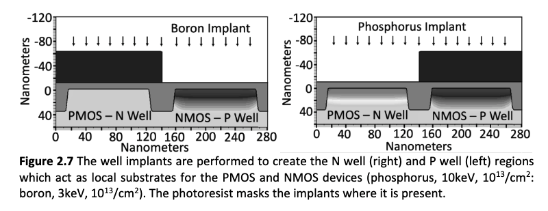
As the NA (the concentration angle) of the lithography increases, you have to use thinner layers of photoresist, lest you have inward sloping edges because of light angle. Thin resist can't block high energy well implants.
In dry etching, chemical reactants are shot at the wafer where they react and remove material. In wet etching, the wafer is submersed in a liquid etchant that removes material. Dry etching is typically more directional than wet etching.
DUV masks are transmitting, meaning they selectively transmit or absorb light based on the pattern. Since every material absorbs EUV light, this approach cannot be used in the EUV case. Instead of transmitting, EUV masks must be reflective in the regions where the resist should be exposed.
1. EUV masks are reflective, so the blank mask must be made of 40-50 alternating layers of silicon and molybdenum. This structure is hard to fabricate. 2. Patterning the mask requires a dedicated multi-beam electron lithography tool. Inspecting the mask for defects requires another dedicated high-resolution inspection tool. Mask yield is ~50% which increases cost. 3. To keep dust particles off the mask, a pellicle must be placed over the mask which must be ultra thin and temperature resilient.
2D materials improve the ability to turn the transistor on and off. Since the 2D material is very thin, the gate material is very close to the charges in the channel and can control them more easily.
- Making contacts to 2D materials is hard. Since they are so thin, the metal contact has to fuse with a thin layer of atoms, which is a difficult chemistry problem.
- 2D materials are very delicate. Their small thickness means small perturbations during manufacturing can ruin the material.
- Different materials have to be used for the NMOS and PMOS channels. There isn't a single 2D material that would work for both cases, so two different materials have to be used.
Further reading
General semiconductor background
- How do Transistors Build into a CPU?YouTube
- Integrated Circuit Fabrication by Plummer and Griffinplummergriffinbook.stanford.edu
Gate-all-around transistors
Industry history and economics
- Intel’s Reign of TerrorYouTube
- The 3-D Transistor TransitionYouTube
- Intel Should Raise CapitalSemiAnalysis
Packaging
Fabrication technologies
- What ASML Has Next After EUVYouTube
- The Extreme Engineering of ASML’s EUV Light SourceYouTube
- Multi-Patterning Techniques: Enabling Dimensions Beyond Lithography Resolution LimitsYouTube
- Engineering the Gate-All-Around TransistorYouTube
- Applied Materials’ Pattern-Shaping TechnologyYouTube
- Embracing Chaos: The Imperfect Art of Semiconductor Manufacturing And LithographySemiAnalysis